
 Image 1 of 20
 Image 2 of 20
 Image 3 of 20
 Image 4 of 20
 Image 5 of 20
 Image 6 of 20
 Image 7 of 20
 Image 8 of 20
 Image 9 of 20
 Image 10 of 20
 Image 11 of 20
 Image 12 of 20
 Image 13 of 20
 Image 14 of 20
 Image 15 of 20
 Image 16 of 20
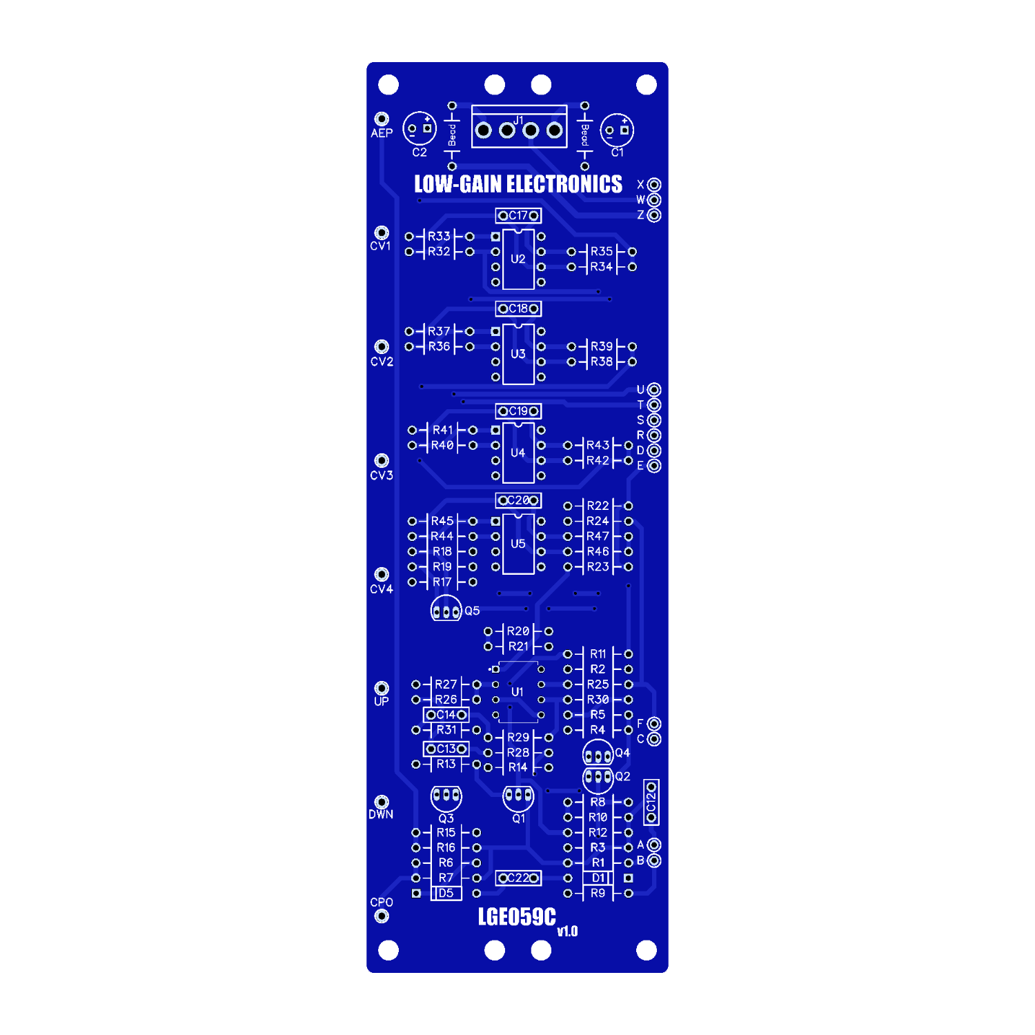 Image 17 of 20
 Image 18 of 20
 Image 19 of 20
 Image 20 of 20
Multi-Stage Programmable Sequencer
4 rows of CV ranging 0-8V output
Stage Address Inputs
Stage Gate Outputs
Dedicated Up and Down advance inputs
Common Pulse Output - Outputs a gate anytime a button is pressed
All Event Output - Outputs a Gate anytime stages change
Stage Address Buttons
LGE059 = stage pcb
LGE059C = Output Buffer PCB
To build with the panel available 5 LGE059 PCB’s are required. (8 Stages would be 8 LGE059 PCB’s)
The sequencer can be built with any number of stages (LGE059 pcb’s). The panel currently available is for a 5 Stage version.
** 4U Modular is a term used for the format most commonly known as “Serge Format” or “Loudest Warning Format”. Out of respect for the ever growing format, 4U Modular is the easiest way to refer to it. More Specifically it refers to the panel height and mounting hole style. 4U Modular will patch up just fine with other 4U "Serge" formats such as "Random Source", but it will not mount in RS boats or Buchla Boats (or power off Buchla power for that matter). An info page about this will be added to the website soon to make this a lot more easy to understand.
Build Documentation:
LGE059-4 Stage Main PCB
LGE059-4 Bill of Materials
LGE059-4 PCB Layout Top w/ Designators
LGE059-4 PCB Layout Bottom w/ Designators
LGE059-4 Schematic
LGE059-4 Panel Art
White Panel (Range Switches)(Single Stage PCB)
LGE059 Bill of Materials (Single Stage PCB)
LGE059 PCB Layout w/ Desginators
LGE059 Schematic
LGE059C V3 Output Buffer PCB Bill of Materials
LGE059C V3 Output Buffer PCB Layout w/ Designators
LGE059C V3 Output Buffer PCB Schematic
LGE059D Buffer I/O PCB Bill of Materials
LGE059D Buffer I/O PCB Layout w/ Designators
LGE059D Buffer I/O PCB Schematic
Blue Panel (no range switches) (Single Stage PCB)
LGE059 Bill of Materials (Single Stage PCB)
LGE059 PCB Layout w/ Designators (Single Stage PCB)
LGE059 Schematic
LGE059C Bill of Materials (v1.2: updated 09/18/23, up/down advance fix, output voltage mod, speed stability mod)
LGE059C PCB Layout w/ Designators
LGE059C Schematic (v1.2: updated 09/18/23, up/down advance fix, output voltage mod, speed stability mod)
Mechanical Parts BOM generally required for building Low-Gain Electronics Modules
Details:
PCB Size: 6” x 2”
Current Draw: TBD